MAX8632 PCB Layout Optimization
Abstract: This application note outlines a clear printed-circuit-board (PCB) layout for implementing the MAX8632 integrated DDR power supply.
Overview of the MAX8632
The MAX8632 integrates a synchronous-buck controller to generate VDDQ main rail, a 3A high-speed low-dropout (LDO) regulator that can source and sink current to generate VTT bus termination, and a 15mA VTTR reference buffer. The buck controller drives two external n-channel MOSFETs to generate output voltages down to 0.7V from a 2V to 28V input. The LDO can sink or source up to 1.5A continuous and 3A peak current. The LDO was designed as a terminator for the DDR memory bus where fast transients can be expected. This requires a control loop with high bandwidth and a circuit to match.
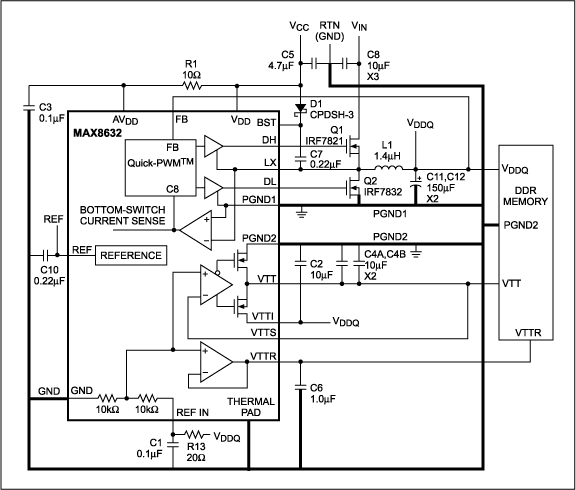
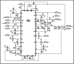
Figure 1. This figure provides a basic block diagram of the MAX8632 integrated DDR memory circuit. The bold lines show the total ground scheme, where current enters at VIN and returns at RTN.
The MAX8632's Ground Scheme
Figure 1 is a simplified block diagram of the MAX8632. It is important to note that there are three separate ground connections on the IC: analog ground (GND), power ground 1 (PGND1), and power ground 2 (PGND2). PGND1 is the power ground for the synchronous-buck controller. This pin functions as a ground sense for the low-side MOSFET (Q2) and also supports the Q2 gate-driver return current. Driver current flows only during switching transitions, which enables accurate current sensing on Q2 at the end of the switching cycle.
Because the VTT supply can have a continuous current through it, PGND2 is not used for sensing. Instead, ground sensing for VTT and VTTR is done at GND, where there is very little current interference, while PGND2 serves only as a power return for VTT (Figure 1). PGND1 is the noisiest section of the ground, but because PGND1 is connected to the RTN trace, the current-sense leads can reject this noise as common-mode noise (the same noise shows up on LX). This configuration allows the Q2 current-sense leads to fly up with the ground bounce. Because current flows from the Q2 source to RTN, very little current flows though the MAX8632 PGND1 pin, allowing accurate current sensing.
Implementing a High-Speed VTT Circuit
Because the MAX8632 circuit must function in the presence of large fast-transient signals, stray components and PCB inductance can reduce performance. This is why C11, C12, and PGND1 are connected to C4A and C4B with the lowest possible inductance trace (i.e. short and wide). Note that power flows from VIN to VDDQ to VTT; then, it flows to PGND2, back to PGND1, and on to RTN. Only a very small chip bias current flows into the analog-ground leg. Voltage feedback for the VDDQ output is sensed at the output terminal and GND. Even though GND is on the other side of the chip, it offers good reference sensing because GND has only one connection to power return and that connection is at the single point where GND and PGND2 meet (see Figure 2). Voltage sensing for VTT has the same basis as VDDQ, and, with C11, C12, C4A, C4B connected together, this GND establishes the system reference ground at this point. VTTR (C6) should also use this as the reference ground. Furthermore, any testing should use this point as a reference, and a test point should be installed here for this purpose.
Because VTT must handle large fast transients, a linear control loop has been deployed in the MAX8632. While switching supplies offer good efficiency, their output inductor limits current slew rate. Current slew rate is limited even in linear circuits, but the slew limiter in this case is lead, and trace inductance is much smaller than a switching supply inductor. Hence, higher transient speeds can be achieved. This is important to keep in mind when laying out the circuit. Using a transconductance output (voltage-controlled current source) can reduce some of the problems that inductance presents. Using a current source as an output raises the output impedance, which has two advantages. First, with increased resistance, the time constant (L/R) for the inductor is reduced. Second, with a high enough output impedance, the second-order pole that is formed by the inductor-capacitor output can be reduced to a single-pole system. In current-mode switching systems, similar attempts are made to reduce the effect of the output inductor. Of course, a linear regulator does not have the efficiency of a switcher, but this is the price that must be paid for high speed.
One other advantage of a high-speed VTT circuit is that the local capacitor can be much smaller. During the time the control loop is ramping current up to meet the load requirements, the output capacitors must supply the load. Therefore, if the VTT driver has a higher current slew rate, the output caps can be smaller. In fact, with a 20µF output cap, 40mV of voltage tolerance, and a 3A peak load transient, we can solve for the slew rate using C * V = Q and knowing Q = I * T.

Or:
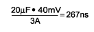
And slew rate equals:
Putting this into perspective, with DDR2 there is 0.9V (1.8V–0.9V) available from the VDDQ rail to drive VTT. The maximum output inductance required to support this speed is calculated with the following equation:

LMAX is 80nH.
This must comprise the trace inductance and the chip, including the bond wires, package, and return ground. In most cases, 80nH can easily be achieved by placing a return ground on the immediate layer under the VTT trace and the VTT output caps and by placing them close to the VTT driver.
Figure 2 provides a simplified layout to illustrate the multiple layers of a real system. In this diagram, power enters at VIN and exits at VDDQ and VTT. With the analog ground (GND) isolated from PGND1, most of the switching noise generated by Q1 and Q2 shows up at VIN and RTN. PGND2 and GND are connected with a single point at PGND2, allowing GND to float on top of the DC errors and noise caused by ground currents.
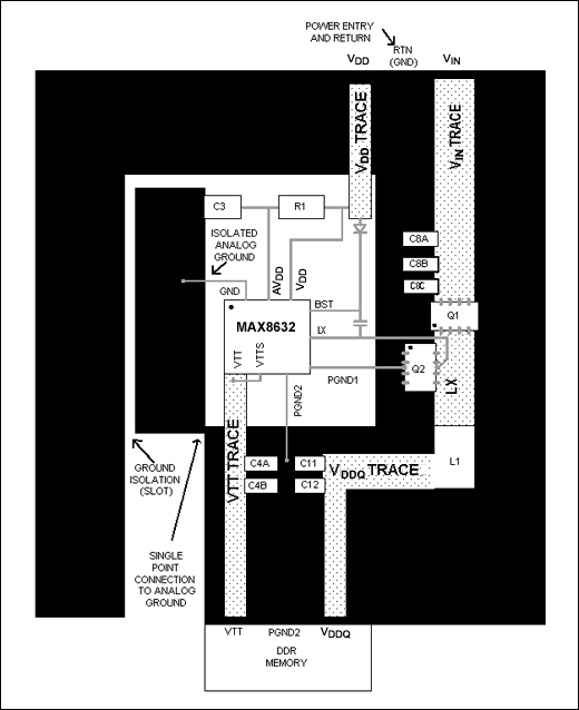
Figure 2. This is a simplified PCB layout for the MAX8632. Notice the isolated analog-ground patch and its single-point connection to PGND2.
A low-noise, 5V bias supply (AVDD) is generated using a resistor-capacitor filter from the 5V VDD input. R1 and C3 filter the noise generated by the boost circuit, and C3 is terminated into GND to reduce noise. R13 and C1 also filter supply noise (see Figure 3)—in this case, the ripple from VDDQ. If the ripple from VDDQ is forwarded to VTT, the LDO will try to drive the 10µF output caps (C4A, C4B). With a 30mV VDDQ ripple and a 300kHz switching frequency, as much as 90mA of current is needed to drive the VTT caps. Because the VDDQ regulator can skip pulses (SKIP), there is less current at light loads. The 80kHz filter formed by R13 and C1 reduces this current to 18mA and, at the same time, allows VTT to dynamically track VDDQ.
Phase Margining
Although the VTT circuit should have sufficient phase margin by moving the feedback point inboard, extra phase margin can be found. This is because some lead phase shift is seen on the lead and trace inductance feeding the VTT output caps. On the other hand, if the feedback point is on the VTT output caps (outboard sensing) some phase margin is lost, but better sensing of output transients and DC accuracy is gained. This configuration allows the circuit to be tuned for optimum performance. The MAX8632 EV Kit has jumper-selectable VTT feedback, which can be seen in the Figure 3 schematic where R16 and R17 select an inboard or outboard feedback point.
Heat Dissipation
The MAX8632 has an exposed pad to help transfer heat from the silicon wafer to the PCB. This metallic exposed pad does not have any electrical connection to the internal circuit. Keeping in mind that the exposed pad must conduct up to 2.68W, it can be tied to any ground. Tying the exposed pad to GND makes a convenient connection to PGND2 and GND (see Figure 5). The middle and bottom planes also connect to the exposed pad (Figures 6, 7, and 8). Notice both that the isolation slot in the ground planes separates PGND1 from GND and PGND2, and also where the grounds are forced to connect. With the ground planes connecting at the exposed pad, they can all conduct heat out of the chip.
Conclusion
Even though time, money, or board space may limit implementation of all the recommendations in this application note, it still offers a good reference design from which to begin.
More detailed image (PDF, 71.3kB)
Figure 3. The MAX8632 Standard EV Kit Schematic.
Table 1. The MAX8632 Evaluation Kit Bill of Materials
| DESIGNATION |
QTY |
DESCRTPTION |
| C1 |
1 |
0.1µF, 10% 16V X7R ceramic capacitor (0603) Taiyo Yuden EMK107BJ104MA |
| C2, C4A, C4B |
3 |
10µF, 10% 6.3V X5R ceramic capacitor (0805) Kemet C0805C106K9PAC or Taiyo Yuden JMK212BJ106MG |
| C3, C6 |
2 |
1µF, 10% 10V X5R ceramic capacitor (0603) TDK C1608X5R1A105K |
| C5 |
1 |
4.7µF, 20% 6.3V X5R ceramic capacitor (0805) TDK C2012X5R0J475M |
| C7, C10 |
2 |
0.22µF, 20% 16V X7R ceramic capacitor (0603) TDK C1608X7R1C224M |
| C8A, C8B, C8C |
3 |
10µF, 20% 25V X5R ceramic capacitor (1210) Taiyo Yuden TMK325BJ106MM TDK C3225X5R1E106M |
| C9 |
1 |
4700pF, 50V X7R ceramic capacitor (0603) Kemet C0603C472K5RAC3946 equivalent |
| C11, C12 |
2 |
150µF, 4V 18m POS capacitor Sanyo 4TPE150MI POS capacitor Sanyo 4TPE150MI |
| D1 |
1 |
Schottky Diode, 30V, 100mA (SOD-323) Central CMDSH-3 |
| JU1, JU2, JU3, JU4, JU6 |
5 |
3-pin header, 0.1in center Sullins: PTC36SAAN (available in a 36-pin strip; place on PCB per example provided) |
| L1 |
1 |
1.4µH, 15.5A , 2.8m power inductor Sumida, CEP125-1R4MC-U |
| Q1 |
1 |
n-channel MOSFET 30V 12m (SO-8) International Rectifier IRF7821 |
| Q2 |
1 |
n-channel MOSFET 30V 4m (SO-8) International Rectifier IRF7832 |
| R18 |
1 |
0 5% resistor (0603) |
| R1 |
1 |
10 5% resistor (0603) |
| R13 |
1 |
20 5% resistor (0603) |
| R2, R3, R4 |
3 |
100k 5% resistor (0603) |
| R5 |
1 |
36.5k 1% resistor (0603) |
| NONE |
5 |
Shunts JU1 (3), JU2 (1-4), JU3 (3-2), JU4 (1-2), JU6 (1-2); Sullins STC02SYAN |
| U1 |
1 |
Integrated DDR Power Supply MAX8632 (5mm x 5mm, 28-pin TQFN) |
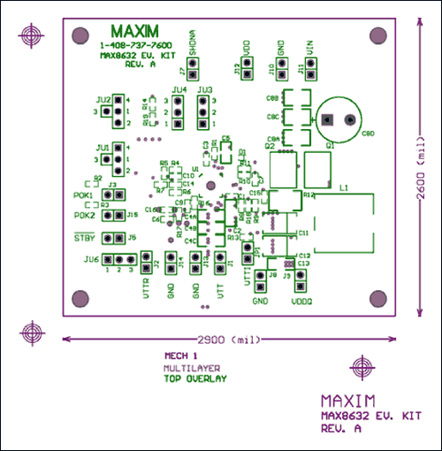
Figure 4. Top-side silk screen.
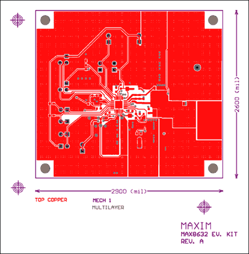
Figure 5. Top-side copper layout.
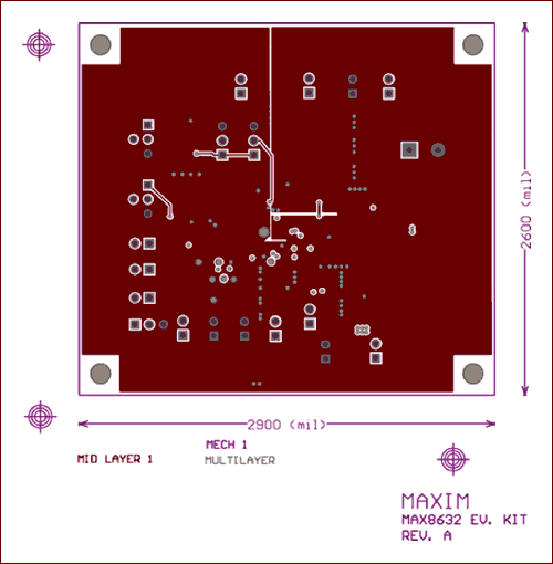
Figure 6. First middle copper layout.
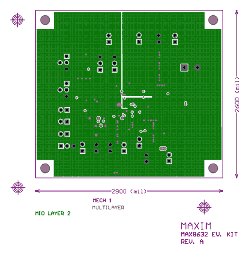
Figure 7. Second middle copper layout.
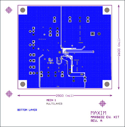
Figure 8. Bottom copper layout.


